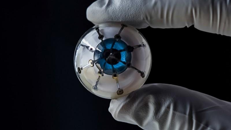
A new 3D-printed bionic eye prototype promises superhuman vision for those who can see and vision for the blind. The research, carried out by a team from the University of Minnesota, suggests that a robotic eye can be fused with the human brain for enhanced vision.
To build this "eye" researchers reportedly made use of a 3D printer, custom made to build their prototype. According to a report by Futurism, researchers first printed out a base layer made of silver particles on the inner side of a glass dome after which semiconducting polymer materials were shaped into photodiodes—a device that converts light into signals—directly onto the silver base.
This entire process, notes the report, only took the team about an hour and by then, the device was able to convert light to electric signals with 25 per cent efficiency. The report points out that the device is not yet ready to be transplanted into a human head just yet. One of the reasons is that a hemispherical glass dome can't be expected to sit comfortably in an eye socket, so researchers are reportedly working on printing soft materials that work just as well.

The device's current efficiency also needs to be scaled up. A human eye is so sensitive that a single photon can be seen clearly, notes the report. This instrument is far off in comparison.
Co-author of the study, Michael McAlpine, however, noted that his team's prototype is still a significant step in the creation of actual bionic eyes, in a release.
Of the many developments, the research has shown that 3D printed semiconductors can be just as, if not better as existing devices manufactured in microfabrication labs—high-tech facilities that have the cutting-edge equipment. 3D printers, notes the report, can do pretty much the same thing using semiconductors even if they do not have access to advanced research facilities. Also, 3D printing allows the arrangement of semiconductors on a curved surface and this is something that is not possible even at advanced microfabrication labs.
The study was first published in the journal Advanced Materials.


